|
|
THE WIEN-BRIDGE THEREMIN
Published October 16, 1999
Updated November 4, 2018
Contents:
Legal
Notice
Acknowledgment
Introduction
Revision
Theory of Operation
Block Diagram and Circuit
Descriptions
Complete Schematic
Circuit Board
Unit Assembly
Parts Tables
Calibration
Procedure
Photos
Legal Notice
(back
to contents)
Information contained in this document ©1999, 2002, 2003, 2014 by Arthur Harrison. It may not be reproduced in any form without his permission, and shall acknowledge him as the copyright holder and author.
Unless specifically stated in a written contract, Arthur Harrison grants no license or permission to any party for the use of the information contained in this document for the manufacture and sale of goods, nor any other commercial utilization. Refer licensing inquiries to: diy@harrisoninstruments.com.
Arthur Harrison assumes no liability for
any damages, direct, or consequential,
which may arise from the dissemination, application, or misapplication
of
the content contained in this site. The User of the information
provided
in this site assumes all responsibility for any damages, direct or
consequential,
which may arise from its use. Arthur Harrison retains the right to
alter
the content within this site at any time without notice.
Acknowledgment
(back to
contents)
The author gratefully acknowledges the
assistance of Wolfgang Wiebach for
his translation of Max Wien's German-language texts from Annalen
Der Physik
und Chemie, and for his assistance in providing biographical
information
about Max Wien.
Introduction
(back to contents)
This circuit is a basic theremin with only a pitch control. It uses the "heterodyne" technique, as did Theremin's original instrument. Heterodyning is advantageous in its simplicity, and is made further attractive in this design by eliminating the coils that are usually hard to find. Although this is a simple theremin without optimized sensitivity and noise characteristics, it is a viable performance instrument.
This project is intended for those with medium to high-level skills in electronics assembly and troubleshooting. An oscilloscope and frequency counter are recommended in the event measurements are required. If you aren't inclined to deal with these issues, commercial theremin kits such as the Minimum Theremin Kit from Harrison Instruments may be a better choice.
When deciding between a "do-it-yourself" or kit-built theremin, be aware that electronic materials can be expensive. Some items can only be purchased in bulk quantities, and many distributors impose "minimum order" requirements. Since it’s unlikely you will find all the parts in one place, also consider the effort required to make many phone calls and write several orders. Of course, if you are equipped with a well-furnished electronics lab, then you may save considerably by building the Wien-Bridge Theremin, using parts you have on-hand.
About Wien
Max Wien was born December 25, 1866 in Königsberg (presently Kaliningrad, Russia). While at the Institute of Physics at the University of Berlin, he developed the two-resistor, two-capacitor frequency-determining network that is used in this theremin's oscillators. Wien published his work in Annalen Der Physik und Chemie in 1891 in the treatise, Messung der Inductionsconstanten mit dem "optischen Telephon" (Measurement of Inductive Constants with the "Optical Telephone"), in which he describes the use of bridge circuits for the precise measurement of capacitance and inductance with an apparatus known as the "Optical Telephone." In the day of Wien's work, there was no electronic amplification; a 1939 adaptation of the Wien network by William Hewlett uses it in conjunction with an automatically-controlled electronic gain system to form a sine wave oscillator.
Wien was a lecturer at the Technical University of Aachen in Germany in 1896, an associate professor at the Technical University of Danzig (now Gdansk in Poland) in 1903, and a full professor at the University of Jena in Germany in 1910. He is also known for his discovery of oscillations in quenched spark gaps and ionization of liquids under the influence of electric fields. He died in Jena, Germany in 1938, where the university's town square is named in his honor ("Max Wien Platz").
(back
to contents)
Revision
(back
to contents)
This circuit was originally designed with a plug-in transformer that provided a ground prong and screw terminal for earth ground. Access to an earth ground terminal is considered advantageous in providing a good electrical coupling between the earth and theremin circuit. That transformer, however, has been discontinued. It has been replaced with a transformer that does not have a ground prong or screw terminal. Accordingly, schematic reference designation for capacitor "C1," which was used in conjunction with the old transformer's ground screw terminal, has been deleted. However, the ground connection between the theremin and earth is still maintained when it is connected to a grounded, mains-operated audio amplifier.
The U1, U2, and U3 dual operational amplifier integrated circuit originally specified, Phillips type NE5532N, has also been discontinued. That IC has been substituted with New Japan Radio equivalent type NJM5532D.
All changes are reflected in the schematics, illustrations, and Parts Tables.(back
to contents)
Theory of Operation
(back to
contents)
Most theremins, including the one in this feature, utilize the principle of "heterodyning," in which two alternating electric signals are combined. If the combining device is a multiplier, the resulting output signal will contain two distinct frequencies, one the sum, and the other the difference, of the input frequencies. For example, if a 1000 Hertz signal is applied to one multiplier input, and a 4000 Hertz signal to the other input, the output will have both (1000 + 4000), or 5000 Hertz, and (4000-1000), or 3000 Hertz frequency constituents. This condition will result if the inputs are both pure sine waves and the multiplier provides an exact multiplying, or "square law," function.
In practice, the multiplier may be substituted with one of several other devices, generically called "mixers." Mixers, however, may produce more than just the sum and difference of two sine wave input frequencies. Also, if the input waveforms are not pure sine waves, the output will contain other frequencies in addition to the sum and difference of the inputs' fundamental frequencies.
There are several types of practical mixers. One common type is the "double-balanced mixer," in which one input signal is alternately multiplied by a positive or negative term, determined by the other input signal. When both input waves to a double-balanced mixer are sinusoidal and limited within certain amplitude bounds, the resulting function is similar to the function of an ideal multiplier. However, if one or both of the inputs contain harmonics, e.g., if they are square waves, or if their amplitudes are relatively high, then the resulting function departs from an ideal multiplier, and the output will contain several other frequencies.
In many applications, including this inexpensive theremin, the precise transfer function of an ideal multiplier is not justified. This instrument's requirements, in fact, can be satisfied with a simplified form of mixer in which one input is simply switched on and off by the other. This technique is a reduced form of the double balanced mixer, in which the alternating-polarity function is replaced with an "on-off," or gating function.
In a heterodyne theremin, the mixer produces outputs that include the difference frequencies of two oscillators, one called the "local oscillator" and the other called the "variable oscillator." In the theremin's "null" condition, during which no audible tone is produced, both oscillators are at the same frequency, so that the mixer's output difference frequency is 0 Hertz. As the variable oscillator shifts in frequency due to the hand's varying proximity, the difference frequency increases from 0 Hertz to an upper limit which is defined by the variable oscillator's maximum deviation from the local oscillator's fixed frequency.
The theremin's antenna serves as one plate of a capacitor. The player's hand functions as the other plate, and as the hand is moved, the value of the capacitance changes in accordance with the distance between the two. For this function to be effective, the body must have an electrical ground commonality with the theremin circuit. While the body is not directly grounded with a wire, its large surface area provides sufficient capacitive coupling to ground (typically about 50pF), and the theremin circuit is grounded through the output cable's shield connection to the grounded audio amplifier. The equivalent electrical model, therefore, includes a large fixed capacitance (between the body and ground) in series with a small motion-modulated capacitance (between the moving hand and antenna).
Since heterodyne theremins, like this design, provide an audible pitch derived from the difference frequency of two high-frequency oscillators, a small percentage of change in either oscillator will cause a large percentage of change in pitch. Therefore, oscillator stability with temperature change and time is important. Wien-bridge oscillators were chosen for these functions because they fulfill these objectives, are easy to build, and do not use coils that are hard to specify and procure.
Although suitably stable, the variable oscillator’s frequency range will not be identical among all units due to component tolerances and lay-out variations. Its frequency range is also affected each time the instrument is moved, because of changes in the proximity of stationary objects near the antenna. To compensate for these variables and the small temperature-induced variable (difficult to eliminate completely), the local oscillator is provided with a frequency control that can be adjusted for nulling the audible pitch for various temperature and position conditions.
As mentioned, heterodyning also produces sum frequencies. In this application, these frequencies, although inaudibly high, are removed prior to the output with a filter. Due to the non-square-law properties of the mixer, certain unwanted audible frequencies, apparent as noise, are also removed by the filter. The specific harmonic quality, or timbre, of the theremin's output partly depends on the filter's characteristics, which, in this design, is a fourth-order implementation incorporating a two-pole Sallen-Key low-pass, a one-pole R-C high-pass, and an integrator. The net filter function provides an output with fairly constant loudness over the instrument's approximate 10kHz range.
|
|
Power
Supply
(back
to block diagram)
|
DANGER ! Lethal voltage is present at the mains outlet and the T1 transformer primary. Observe appropriate high-voltage safety precautions. Never connect the mains wires to any part of the circuit except the T1 transformer's molded-in primary prongs. Observe the polarity of electrolytic capacitors C2, C3 and C4 and rectifiers CR1 and CR2. Connect them only as indicated in the schematic. The improper insertion of components may result in severe personal injury. |
 |
Transformer T1 reduces the mains to an appropriate voltage and provides isolation for safety. CR1 and CR2 provide half-wave rectification of T1's secondary voltage. The positive, pulsed DC voltage at CR1's cathode is filtered by capacitor C2, and applied to the input of voltage regulator VR1. VR1 provides +12 volts for the rest of the circuit. The negative, pulsed DC voltage at CR2's anode is filtered by capacitor C3 and applied to the input of voltage regulator VR2. VR2 provides -12 volts for the rest of the circuit. VR2 has an output capacitor, C4, required for stability.
A two-conductor cable is used to connect the transformer's secondary terminals to power plug P1.
Refer to the "Construction" section for assembly details regarding the transformer and its connecting hardware.
(back to
block diagram)
Variable
Oscillator
(back
to block
diagram)
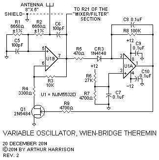 |
Operational amplifier U1B, in association with R1, R2, C5, and C6, form the primary frequency-determining elements of a Wien-bridge oscillator. Discounting antenna capacitance, the theoretical frequency of oscillation is determined by 1/2piRC, where R=R1=R2 and C=C5=C6. In practice, phase shifts occurring in the operational amplifier causes this frequency to be about 12 percent lower than predicted by the formula. In the prototype, the oscillator produced about 216kHz with no hand-induced capacitance, and about 207kHz with the hand one inch from the antenna. Component tolerances and variations in physical construction will cause some unit-to-unit variation in these values.
In a Wien-bridge oscillator, the frequency of operation is determined by the aforementioned formula provided that the DC gain of the amplifier (U1B) is maintained at a level for which the output wave form is sinusoidal. This gain, a value approximating 3.0, is maintained by the remaining circuit components.
Operational amplifier U1A and associated components form a half-wave detector and averaging circuit. This is an AGC (automatic gain control) servo loop which monitors the peak voltage at U1B's output. The time constants for the AGC loop are determined by resistors R5 and R8 and capacitor C8. U1B's output value is compared to the reference voltage at U1A's positive input, provided by the voltage divider comprised of R6 and R7. U1A's output, in turn, controls the gate voltage of N-channel junction field effect transistor Q1. Q1, in conjunction with R3 and R4, form the DC gain-determining components for U1B. The gate voltage, and therefore the channel resistance of Q1, is maintained at whatever value necessary to cause the peak average voltage at U1B's output to equal the reference voltage at U1A's positive input, a value chosen to prevent U1B's output from reaching saturation and ensuring a sinusoidal wave shape. For the +12 volt power supply and the values shown, the reference voltage at U1A pin 5 is about 1.78 volts, the channel resistance of Q1 is maintained at about 6700 ohms, and the peak-to-peak output voltage at U1B is about 5 volts.
An 8" by 5" rectangular metal plate connects to the U1A Wien-bridge circuit at the junction of R2 and C6, and serves as the pitch control antenna for the theremin. Small variations of capacitance caused by variations in the proximity of the hand and antenna affect the oscillator's frequency by changing the value of the capacitance in the frequency-determining network (R1, R2, C5, and C6). The hand-to-antenna capacitance, which varies several picofarads over the approximate 18-inch sensing range, causes the oscillator's frequency to shift about 10kHz downward when the hand is moved near the antenna.
The antenna may alternatively be connected to the positive input of U1A. However, the arrangement shown was chosen to provide an additional degree of isolation, via R2, between the antenna and IC to help protect it from inadvertent static electric discharges.
Capacitors C9 and C10 provide power supply decoupling for U1, and capacitor C7 reduces power supply noise at U1A's reference input. Resistor R9 limits the gate current in Q1 in the event that the output of U1A swings positive.
Variable Oscillators and Interference
In theremins, hand capacitance is one of the determinants for the variable oscillator's frequency. Ideally, it is the only parameter that should modify the oscillator's frequency. However, the antenna, which is part of the hand-capacitance circuit, also provides a means of entry for interfering electromagnetic radiation. Such radiation causes perturbations in the oscillator's signal, and therefore noise in the output.
Referring to line 25 of page two in his U.S. patent, number 1,661,058, Leon Theremin states that "Said element [meaning the variable oscillator's antenna] does not function like the antenna in a wireless receiver set or apparatus, i. e., it does not receive or detect radiant energy..." This of course, is the intention of the antenna's function, although radio frequency interference is, in fact, an issue which must be addressed.
Traditionally, theremin oscillators contain a resonant section comprised of one or more inductors and capacitors. (Theremin, in fact, went beyond incorporating a single resonant section in his variable oscillator, and introduced a "compound" control which improves the instrument's sensitivity.) Oscillation is sustained by amplification and positive feedback at a frequency determined by these components. "Q," or "Quality factor" is a quantitative characteristic of a resonant network that is related to the number of cycles the network will produce from an impulse excitation before the amplitude of its oscillation diminished to a given percentage of its original value. A high Q control will resist oscillation when subjected to influences that occur at frequencies different from its inherent resonant frequency, for example, those occurring in interfering electromagnetic radiation.
This theremin uses a Wien-bridge oscillator that has resistors and capacitors instead of inductors and capacitors as frequency-determining elements. This was done to promote simplicity, since resistors and capacitors are less expensive and more commonly available than inductors. The phase selectivity implicit in the Wien network causes oscillation at a specific frequency, therefore limiting the influence of interfering electromagnetic radiation.
(back to
block diagram)
Local Oscillator
(back to block
diagram)
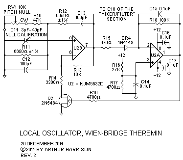 |
The local oscillator is a Wien-bridge type, practically identical to the variable oscillator, but with no antenna, and with two variable controls: Potentiometer RV1 and variable capacitor C11. This oscillator provides the reference frequency that the variable oscillator beats against. The variable controls permit the user to "null" the theremin to a zero beat when the hand is away from the antenna. Since the local oscillator and variable oscillator are similar, temperature-induced frequency drift in the beat frequency is largely canceled.
RV1 should be located a reasonable distance from the antenna, since the hand's presence would otherwise cause an offset during the pitch-nulling procedure.
(back to
block diagram)
Mixer/Filter
(back
to block
diagram)
|
DANGER ! Do
not play this instrument at a high volume, Use
headphones that have a built-in volume control, |
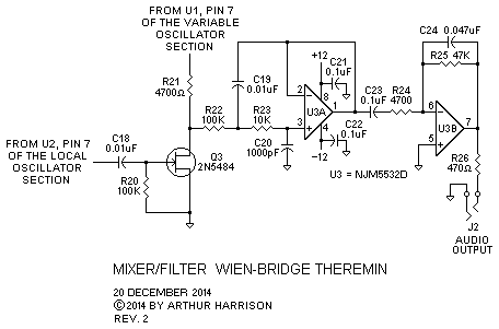 |
The sinusoidal output from the variable oscillator is applied to the top of R21. The sinusoidal output from the local oscillator is applied to the gate of Q3, a depletion-mode, N-channel, junction field-effect transistor, via C18. When the voltage at Q3's gate exceeds its Vgs(off) threshold, it turns on, shunting the signal at the junction of R21 and R22 to ground. With the gate negative, Q3 turns off, allowing the signal to be present at R22. Heterodyning, which results from the gating of the variable oscillator output by the local oscillator output, takes place at the junction of R21 and R22.
U3A, in conjunction with R21, R22, R23, C19, and C20, form a Sallen-Key low-pass filter. This filter passes the audible, difference frequency of the two oscillators, and removes the inaudible sum frequencies. The output of the filter, U3, pin 1, is AC coupled via C23 to an inverting gain stage consisting of U3B and associated components. R24 and R25 establish the dc gain for this stage. C24, in conjunction with R25, determine the high-frequency roll-off, and C23, in conjunction with R24, establish the low-frequency roll-off of the U3B section. Resistor R26 isolates U3B’s output from load capacitance and serves as a current limiter. Capacitors C21 and C22 provide power supply decoupling for U3.
The maximum audio output amplitude is about 2.5 volts peak-to-peak, and occurs at a frequency of about 170 Hertz. The output amplitude rolls off to about 1.25 volts peak-to-peak at about 30 Hertz and 1000 Hertz.
Important Note: This theremin's output is considerably greater than the outputs from most instruments. Use the "line level" input of external amplifiers, and start with the volume control at the minimum position. Be certain that the theremin is producing an output tone, and then slowly raise the volume on the amplifier.
|
|
Circuit Board
(back to
contents)
|
SAFETY NOTICE: Some of the components used in this construction are "polarized," which means that they will only function properly when inserted into the circuit in the right direction. Always observe component polarities carefully, and double-check the orientation of transistors, diodes, integrated circuits and polarized capacitors before applying power to any circuit. Reverse insertion of an integrated circuit, a common error, will usually ruin it. Do not reuse a part which has been subjected to improper insertion. As noted in the Power Supply section, reverse insertion of rectifiers CR1 and CR2 or capacitors C2, C3, or C4 can cause overheating and explosions. Always wear safety glasses when using tools and materials. |
| A) | . | General Information |
| 1. | Overview | |
| 2. | About Lay-out | |
| 3. | Soldering | |
| B) | . | Materials and Components |
| 1. | Board, Terminals, Wire, Sockets | |
| 2. | Shields | |
| . | 3. | Semiconductors |
| . | 4. | Capacitors |
| . | 5. | Resistors |
| 6. | Potentiometer | |
| . | 7. | Antenna |
| . | 8. | Output Jack |
| . | 9. | Transformer and Connecting Hardware |
| C) | . | Lay-out Drawings |
| . | 1. | Top View |
| . | 2. | Bottom View |
A) General Information
1. Overview
(back to
section index)
This section contains useful, detailed information for the construction of the Wien-Bridge Theremin circuit board, including top and bottom lay-out drawings. Adherence to the advice in this section is important and strongly recommended.
The circuit board is constructed using "point-to-point" wiring, with all the components and the ground bus wires mounted on the top side, and the remaining wires on the bottom side. The board is arranged in four sections, corresponding to the four functional circuit blocks.
The variable and local oscillator sections are diagonally separated to prevent unwanted coupling. Within sections, leads are kept as short as practical to prevent the pick-up of extraneous signals.
There are two flat shields, one above, and one below, the
circuit board.
A suggested arrangement for the circuit board, circuit board shields,
antenna,
jacks, and nulling control is provided in the "Unit Assembly" section.
2. About Lay-out
(back
to section
index)
In an electronic circuit, the relative positions of components and the configuration of the wires that connect them is called its "lay-out." Lay-out is an important factor that directly affects a circuit’s quality of performance, because:
Components and conductors radiate energy in the form of electrostatic and electromagnetic fields that exert an influence on everything around them. Components are "coupled" by these fields’ influences, sometimes causing undesirable interactions between different sections of a circuit. When this happens, shields, physical separation, or both, must be used to prevent undesirable coupling.
Electronic components are interconnected with conductors such as leads, wires, printed circuit foil, and solder. Conductors are not "perfect" because they have the properties of resistance and inductance which alter the characteristics of the current passing through them. Sometimes, these "parasitic" qualities have to be reduced by using conductors with large cross-sections (to reduce resistance) and by limiting their lengths (to reduce inductance and resistance).
The oscillators in this theremin use relatively small, 100 picofarad, capacitors. Excessively long wires, if improperly positioned, will introduce substantial additional capacitances into the oscillator circuits. Such capacitances, referred to as "strays," may inhibit proper operation. Therefore, it is important to keep the connections direct, and to avoid long, sloppy loops of wire.
3. Soldering
(back
to section
index)
Components can be damaged or degraded from excessive heat, so care should be taken when soldering. Use a 30 to 50 watt, 700°F, thermostatically controlled soldering "pencil" with 22 gauge, 63% tin, 37% lead alloy, rosin core solder. Never use acid core, zinc chloride, or plumbing solder. Terminals and leads must be absolutely clean and free of oxides. If you’ve never soldered, ask someone with experience to teach you the proper technique, and practice first.
Before you solder a connection, be sure that the items being connected are in physical contact with each other. In this project, most of the component leads are placed between the two tines of fork terminals. Although there is no need to wrap the leads around the fork, be sure that the lead is properly nested prior to soldering, and long enough to protrude slightly beyond the fork. Although wrapping the lead around the fork or crimping the fork closed will improve the likelihood of a good connection, doing so makes component removal very difficult, should the need arise.
Be sure there is no residual coating material from the body of the component in the area to be soldered. This problem frequently occurs with conformally-coated resistors, especially when the soldered connection is made close to the component body.
B) Components
1. Board, Terminals, Wire, Sockets
(back to
section index)
Most of the parts are mounted on a sheet of material commonly called "perfboard." The perfboard in the parts list, Vector type 84P44WE, is made of a sturdy glass-epoxy material which resists cracking. Phenolic and paper-epoxy type boards are not recommended, because they are more fragile. The perfboard is furnished with a matrix of 0.042" diameter holes on 0.1" centers. The item listed has 84 columns by 44 rows of holes, and is cut to a size that has 61 by 44 holes, which is 6.2 x 4.5 inches.
The board may be cut by deeply scoring along a column of holes with an awl, and then breaking it along the score. If you use this technique, clamp the board and a straight-edge guide securely to a sturdy work surface. You will need 61 columns of holes across, so score and break the material along the 62nd column. Once the board is cut to the proper size, use the "Top View" to locate and drill the four 0.140"-diameter mounting holes.
The Vector T68A terminals are pushed into the top side of the perfboard, where needed, to provide junctions for component leads and wires. The terminals are inserted with long-nosed pliers. They can be quite hard to push in. If so, use a slight alternating clockwise-counterclockwise twisting motion while you push. Make certain that each terminal is securely and squarely seated. One end of the T68A terminal is a two-tined fork, and accepts one or more component leads (or top-side wires). The other end is a square cross-section pin, designed to accept a "Wire-Wrap®" connection.
The Vector T68A terminals are quite costly. They are only sold in packages of 1000 for $103.25. Unless the builder routinely requires these terminals for several projects, this will probably be considered an unreasonable expense. To reduce cost, the Vector type T68 terminal, which has a longer tail than the "A" version, may be used. The T68 is less expensive at $66.10 per thousand, and they are also available in packages of 100 for $10.71. (The author prefers the shorter terminal, since it permits the fabrication of more compact assemblies.)
Note: If the T68 terminals are used instead of the T68A types, the length of the four threaded standoffs located between the lower shield and circuit board will have to be changed from 1/2" to 3/4" to accommodate the longer terminals' tails. Alternatively, the tails of the T68 terminals may be trimmed to a shorter length.
Wire-Wrap® is a technique for making rapid, solderless connections. If you do not have Wire-Wrap® tools, the bottom-side connections may be soldered, instead. Before you solder to the pin ends of the terminals, first cut them to a length of 1/4". This will provide space for pliers and the soldering iron tip. The solid conductor, tinned, 26 gauge Kynar® insulated wire specified in the parts list can be either wrapped or soldered. Tefzel® or Teflon® insulated wire may also be used. It is less likely to melt from normal soldering temperatures, but it is harder to strip than Kynar®. A wire with a tinned conductor is desirable, because it solders much more easily than bare copper, which tends to oxidize quickly.
A wide braid material, normally used for desoldering, is used for the top-side ground "bus." This thick conductor minimizes voltage differences from one ground point to the other. Note that the braid is placed against the edge of the terminals without wrapping or crimping. Make sure that the braid is pushed directly up against the terminal, and inspect each connection carefully to ensure that it is securely bonded after soldering.
There are two short jumper wires on the top side of the board, located at the VR1 and VR2 regulator outputs. Use bare Wire-Wrap® wire for these two connections.
Teflon-insulated, 22 gauge, stranded "hook-up wire" is specified for connecting the board to peripheral components; J1, J2, RV1, and the antenna.
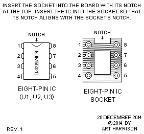
This instrument uses three eight-pin sockets, one each for ICs U1, U2, and U3. The sockets are equipped with square cross-section Wire-Wrap® pins that are inserted through the board. Like the fork terminals, these pins may be cut to a length of 1/4" if soldering is used instead of wrapping. Typically, both the ICs and the sockets have a feature, such as a notch, to indicate the correct orientation of the inserted IC. The figure below shows the correct orientation of the ICs and sockets.
 |
2. Shields
(back to section
index)
Two identical conductive shields are used in this instrument, one above and the other below the circuit board. The shields prevent the signal on the antenna from coupling into the local oscillator. This is advisable, since such coupling will otherwise adversely affect the theremin's fidelity in the lower-pitch range, and may also reduce the instrument's sensing range.
Each shield's dimensions are the same as the circuit board's, 6.2 inches by 4.5 inches. They may be made from any thin conductive material, such as the single-sided copper-clad material commonly used for printed circuits. Double-sided clad board will work equally well.
Each shield requires four corner mounting holes that are precisely aligned with the circuit board's mounting holes. Before mounting any components on the circuit board, use the blank board as a drilling template to locate these holes. One of the shields will require an additional hole that aligns with the adjustment stud on the C11 variable capacitor. It is advisable to locate that hole (at the 41st row and 30th column) using the blank board as a template, as well. If single-sided copper-clad material is used, arrange them so that their copper surfaces face inward, toward the circuit board.
The shields must be electrically connected to the circuit's
ground. This
is accomplished with the use of a solder lug that is positioned at the
board's
upper left mounting hole. The lug contacts the metal spacer that
supports
the upper shield, grounding the shield. The lower shield is
grounded
through the respective mounting screw. The lug is connected to the
circuit's
ground with a short length of top-side wire going to the upper left
terminal.
Bare Wire-Wrap® wire may be used for this purpose.
3. Semiconductors
(back to
section index)
Oscillator integrated circuits U1 and U2 are New Japan Radio NJM5532D dual bipolar operational amplifiers, selected for their high gain-bandwidth product (10MHz) and output drive capability. The NJM5532D also exhibits small phase-gain variations over temperature, important in limiting temperature-induced frequency drift. Another candidate for U1 and U2 is the National Semiconductor LM833N. Since U1A and U2A require a relatively high gain-bandwidth, most dual operational amplifiers, including the ubiquitous '1458, will not work because it is too slow. Some JFET-input types such as the National LF353N or Texas instruments TL072CP will work except for much greater temperature drift, as well as a further departure from the predicted frequency of oscillation.
Mixer/Filter integrated circuit U3 is also specified as a NJM5532D, but requirements are much less critical in this section. Here, many dual operational amplifiers will work as substitutes, including the National LF353N, LM833N; Texas Instruments TL072CP, TL082CP; or Motorola (On Semiconductor) MC1458CP1.
When ordering integrated circuits, pay careful attention to the part numbers. The types used in this construction are housed in "dual-in line" packages. However, the same devices are are also furnished in "small outline" packages, intended for automated printed circuit fabrication, and these variants can not be easily socketed. The difference between part numbers may only be a single letter or digit.
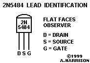
The 2N5484 N-channel junction field-effect transistor (JFET) used in positions Q1, Q2, and Q3 was selected for its low Vgs(off) threshold characteristic of -3.0v, maximum, and should not be randomly substituted. The following figure identifies the leads for this type. In the lay-out, Q1 and Q2 are mounted with their flat surfaces down, and Q3 is mounted with its flat surface up.
 |
The 1N4001 rectifiers CR1 and CR2 may be substituted with any one-half to two-ampere silicon types, including 1N4002 through 1N4007, 1N4933, 1N5391, or 1N5400.
The 1N4148 diodes CR3 and CR4 may be substituted with most switching types, including 1N914, 1N4448, and 1N4531.
VR1 and VR2 are standard "TO-220"-packaged voltage regulators. Although they are capable of providing more current than needed in this application, the use of smaller regulators, supplied in miniature "TO-92" packages, is not recommended.
When wiring VR1 and VR2, pay careful attention to their lead designations, which differ between the two types. Make sure they are oriented with their metal tabs flat against the board. Note that the tabs are electrically connected to the center pin on each regulator; therefore, VR1's tab is at ground and VR2's tab is at the unregulated negative voltage level. So, do not allow the regulators' tabs to touch each other or any other conductors.
The following list of equivalent types is provided for substitutions:
|
|
|
4. Capacitors
(back
to section
index)
Capacitors C2, and C3 are 470 microfarad aluminum electrolytic types. They may be substituted with units that have a greater number of microfarads, but be sure that they are rated at least 25 volts. Also, be sure that substitute capacitors do not exceed a diameter of 1/2 inch, the distance between the board top and the top shield.
C4 is a tantalum electrolytic capacitor, chosen for its small size and low impedance. It may be substituted with an equally rated, miniature aluminum electrolytic capacitor, if desired.
C5, C6, C12, and C13 are 100 picofarad, ±5% tolerance mica capacitors, preferred for their superior temperature stability. "C0G" ceramic or polystyrene types will also work in these four positions.
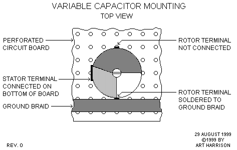
C11 is a miniature polypropylene variable type with an adjustment range of 3 to 40 picofarads. Note that C11 is not soldered to terminals, but instead, pushed directly through the circuit board's holes. Two of C11's terminals are internally connected to the "rotor" of the capacitor (the part that turns). One of the two rotor terminals is connected to the circuit's top-side ground bus by means of soldering, and the redundant rotor terminal is left unconnected.
C11's third terminal is connected to its "stator." This terminal is connected to resistor R10's top terminal with a wire on the bottom of the board. Since the stator terminal is not suited for wrapping, one end of the wire is soldered to it, and the other end is wrapped to the R10 terminal. The following figure shows how C11 is mounted.
 |
The remaining capacitors, 1000 picofarad, 0.01 microfarad,
0.047 microfarad,
and 0.1 microfarad, are general-purpose "X7R" ceramics. The 0.1
microfarad
units should be small enough to fit conveniently near the IC sockets to
facilitate short connections to their power supply pins and the ground
bus
braid. Note: The inexpensive ceramic capacitors specified are
very
delicate when their leads are heated from soldering. Do not attempt to
reposition
these capacitors while their leads are hot, as they will crumble
easily.
These units are sufficiently rugged at normal temperatures.
5. Resistors
(back
to section
index)
There are two types of resistors used in this circuit. One is the general-purpose, ±5% tolerance carbon film type and the other is the ±1% metal film type. The metal film resistors are used where stability over temperature change is important, or where the value of the resistance must be very specific. For this circuit, you may substitute any of the ±5% resistors with the closest-valued ±1% resistor, however, do not replace the ±1% resistors with ±5% parts.
Resistor wattage generally relates to size. The wattage rating
for
commercial-grade parts is specified for a temperature of 25°C. 1/4 watt
units are usually about 1/4" long and 1/10" in diameter, excluding
leads.
Smaller, 1/8 or 1/10 watt resistors may substitute the 1/4 watt units
specified.
6. Potentiometer
(back
to section
index)
RV1, the 10k ohm, linear taper pitch-nulling potentiometer, is a high-quality unit with a conductive-plastic element. Conductive-plastic potentiometers offer superior settability compared to carbon units. However, if cost is a consideration, then a less expensive, carbon potentiometer such as the Mouser stock number 31VA401-F3 may be used as an alternative.
The Clarostat type 53C110K specified has a 2"-long metal shaft that may be cut to the desired length. For the prototype, the shaft was cut to a length of 5/8".
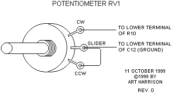
The potentiometer has three terminals, designated "clockwise" (CW), "slider", and "counterclockwise" (CCW). The figure below indicates RV1's connections to the circuit board.
 |
7. Antenna
(back to
section index)
The antenna plate may be made of any metal. The prototype's antenna is made from the 1/16th-inch thick, single-sided copper-clad material commonly used for printed circuits, with the insulated surface facing upward toward the hand. Double-sided clad board will work equally well. In the prototype, a wire was soldered to the clad surface of the material and connected in a direct path to the perfboard. A direct path helps eliminate parallel "stray" capacitance from affecting the circuit. If desired, the wire may be connected to the antenna with a crimp terminal, machine screw, and nut to facilitate disassembly.
The antenna may be substituted with any number of forms. You
may want to
experiment with variations. The specified shape, however, was chosen to
provide
a good hand-sensing distance. If you change the size or shape of the
antenna,
or its proximity to surrounding objects, the frequency of the local
oscillator
may have to be modified accordingly by changing the values of
frequency-determining capacitors C12 and C13. Rod antennas, like the
ones
used in traditional theremins, are not recommended, since they do not
have
an adequate surface area for permitting effective capacitive coupling
to
the hand.
8. Output Jack
(back
to section
index)
J2, the output jack, may either be the monophonic, 2-conductor type indicated in the schematic, or a stereo, 3-conductor type (listed as "alternative J2") in the Parts Table. Most modern headphones are stereo. If you intend to use this theremin only with stereo headphones, use the stereo jack. If so, wire the "tip" and "ring" terminals of the jack together and connect them to R26. Connect the "sleeve" terminal to ground. If you do this, remember that a monophonic patch cord will not work, since its plug will connect the ring and sleeve contacts together when inserted into the jack, short-circuiting the theremin’s output to ground. (This will disable, but not damage it.)
If you plan to connect the theremin to a mixer, effect box, or power amplifier, the monophonic jack should be used. Connect the monophonic jack’s "tip" terminal to R26 and its "sleeve" terminal to ground. Use a standard, monophonic, 1/4" "guitar" patch cord to connect the theremin to the auxiliary device.
Important Note: If the theremin is constructed with a 3-conductor stereo headphone jack, and connected to the 1/4"-phone jack "balanced" input of a mixing board with a 3-conductor stereo patch cord, little or no amplification will result. This is because the signals at the "tip" and "ring" of the cord will be in phase, and therefore cancel each other in the balanced input circuit of the mixer. If you intend to connect your instrument to a mixing board equipped with 1/4"-phone jack balanced inputs, be certain to construct the theremin with a monophonic, 2-conductor jack, and use a monophonic "guitar" patch cord. With this arrangement, one of the mixer's two balanced inputs will be grounded, and the other input will receive the theremin's output signal.
You may also equip the theremin with one of each type of
output jack so that
both headphones and/or an external amplifier may be used.
9. Transformer
and Connecting
Hardware
(back to
section index)
The Hammond transformer, T1, has two screw terminals.
The cable specified in the Parts List has two insulated conductors; a red wire and a black wire. Each wire connects to one of the transformer's screw terminals.
The wires are connected to the transformer’s binding screws with crimped ring terminals. These terminals provide stress relief for the conductors, and will prevent them from breaking.
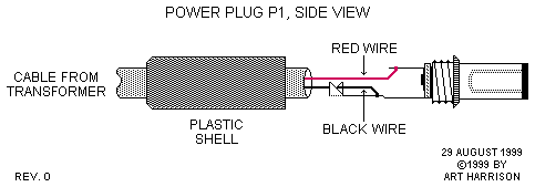
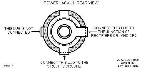
The other end of the cable is connected to coaxial power plug P1. The black cable wire is connected to the lug that goes to P1's outer contact surface, and the red cable wire is connected to the lug that goes to P1's inner contact surface.
P1 plugs into power jack J1 on the instrument. Two of J1's solder lugs are connected to the circuit board. J1 has a third lug that is not connected.
Important note: A "phone" type plug and jack should not be used for P1 and J1, because phone plugs will short-circuit when partly inserted, causing the transformer to overheat.
The figures below provide details of the transformer, cable, plug and jack.
 |
 |
C) Lay-out Drawings
|
|
(back to
section
index)
BOTTOM
|
|
Unit Assembly
(back to
contents)
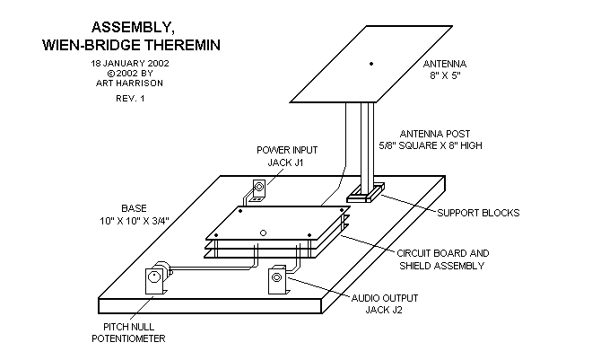
There are several options for configuring the circuit board assembly, its peripheral parts, and the antenna. This section describes the method used for the prototype, which is unenclosed for simplicity. Enclosed configurations are also viable, and left to the builder's discretion.
The first figure illustrates an overall view of the instrument. A 10" x 10" x 3/4" thick piece of wood is used for the instrument's mounting base. Clear pine was used for the prototype, although any good-quality wood, free of knot holes and dimensionally square, will suffice.
The antenna is attached to an eight-inch-high pine wood post with a number 6 x 1" pan-head sheet-metal screw. The post is attached to the base with a number 6 x 1 1/2" flat-head sheet-metal screw (not shown in the figure), inserted through the bottom of the base. This permits removal of the antenna for storage, however, if desired, the post may also be glued in place. Drill pilot holes in the post before inserting screws to prevent it from splitting. The bottom of the post is framed with four wood support blocks that keep it perpendicular to the base and prevent it from rotating. These blocks are glued in place.
The pitch nulling potentiometer and the two jacks are mounted on right-angle metal brackets, each secured to the base with two #6 x 1/2" pan-head sheet-metal screws. The brackets are made of 1/16"-thick aluminum or other suitable metal. Their exact dimensions are left to the builder. If you use aluminum, select an alloy that doesn’t crack when folded. If you don’t have a sheet metal brake, use a sturdy, well secured vise to hold the pieces at their bend lines, and a block of wood to push them into "L" shapes. The holes required for the potentiometer and jacks are quite large, so you should drill them before folding. When drilling, clamp the pieces firmly in a vise.
 |
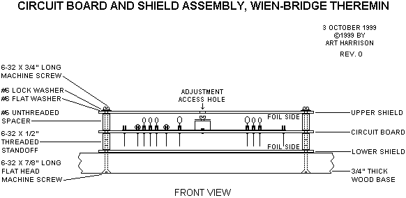
The next figure is a detailed, front view of the circuit board and shield assembly. The spacers, standoffs, and associated hardware is duplicated for the back of the assembly (not shown in the figure).
 |
Parts Tables
(back to
contents)
| Mouser | http://www.mouser.com/ |
| Harrison Instruments | http://harrisoninstruments.com/ |
| McMaster-Carr | http://www.mcmaster.com/ |
| Weico | http://www.weicowire.com/ |
| ITEM | DESCRIPTION | VALUE | MANUFACTURER | MANUFACTURER PART NUMBER |
SUPPLIER | SUPPLIER STOCK NUMBER |
QTY & PRICE |
| C1 |
ITEM DELETED |
- |
- |
- |
- |
- |
- |
| C2, C3 | ALUMINUM ELECTROLYTIC CAPACITOR |
470 uF ±20%, 25 V, AXIAL, 10mm D x 18mm L |
VISHAY /BC COMPONENTS |
MAL202126471E3 | MOUSER | 594-2222-021-26471 | 2@ 1.36 EACH |
| C4 | TANTALUM ELECTROLYTIC CAPACITOR |
10 uF ±10%, 25 V, RADIAL |
VISHAY/ SPRAGUE |
199D106X9025C1V1 |
MOUSER | 74-199D106X9025CA1 |
1@ 1.29 EACH |
| C5, C6, C12, C13 |
MICA CAPACITOR |
100 pF ±5%, 500V, RADIAL |
CORNELL DUBILIER /CDE |
CD15FD101JO3 | MOUSER | 5982-15-500V100 | 4@ 2.04 EACH |
| C7, C8, C9, C10 C14, C15, C16, C17, C21, C22, C23 |
CERAMIC CAPACITOR |
0.1 uF ±10%, X7R, 50 V, RADIAL, 2.5mm LEAD SPACE |
VISHAY/ BC COMPONENTS |
K104K15X7RF53L2 | MOUSER | 594-K104K15X7RF53L2 | 11@ 0.17 EACH |
| C11 | POLYPROPYLENE VARIABLE CAPACITOR |
3 TO 40 pF | SPRAGUE/ GOODMAN |
GYC40000 | MOUSER | 659-GYC40000 | 1@ 7.34 EACH |
| C18, C19 | CERAMIC CAPACITOR |
0.01 uF ±10%, X7R, 50 V, RADIAL, 5mm LEAD SPACE |
VISHAY/ BC COMPONENTS |
K103K15X7RF5TH5 | MOUSER | 594-K103K15X7RF5TH5 | 1@ 0.29 EACH |
| C20 | CERAMIC CAPACITOR |
1000 pF ±10%, X7R, 100 V, RADIAL, 5mm LEAD SPACE |
VISHAY /BC COMPONENTS |
K102K15X7RH5TH5 | MOUSER | 594-K102K15X7RH5TH5 | 1@ 0.19 EACH |
| C24 | CERAMIC CAPACITOR |
0.047 uF ±10%, X7R, 50 V, RADIAL, 2.5mm LEAD SPACE |
VISHAY /BC COMPONENTS |
K473K15X7RF53L2 | MOUSER | 594-K473K15X7RF53L2 | 1@ 0.39 EACH |
| CR1, CR2 |
RECTIFIER | 1 A, 100 V, DO-41 AXIAL CASE |
RECTRON | 1N4002-B | MOUSER | 583-1N4002-B | 2@ 0.21 EACH |
| CR3, CR4 | DIODE | 200 mA, 75 V DO-35 AXIAL CASE |
FAIRCHILD | 1N4148 | MOUSER | 512-1N4148 | 2@ 0.10 EACH |
| J1 | JACK, POWER, COAXIAL |
2 CONDUCTOR, 0.1" DIA.CENTER PIN |
SWITCHCRAFT | 712A | MOUSER | 502-712A | 1@ 2.48 EACH |
| J2 | JACK, PHONE | 1/4" MONOPHONIC, INSULATED |
SWITCHCRAFT | N111X | MOUSER | 502-N111X | 1@ 2.34 EACH |
| ALTERNATIVE J2 (see highlighted text) |
JACK, PHONE | 1/4" STEREO, INSULATED |
SWITCHCRAFT | N112BX | MOUSER | 502-N112BX | 1@ 5.56 EACH |
| P1 | PLUG, POWER, COAXIAL |
2 CONDUCTOR, 0.218" OUTSIDE DIA., 0.1" INSIDE DIA. |
SWITCHCRAFT | 760 | MOUSER | 502-760 | 1@ 2.75 EACH |
| Q1, Q2, Q3 |
TRANSISTOR, JUNCTION FIELD-EFFECT |
N-CHANNEL, TO-92 CASE |
FAIRCHILD | 2N5484 | HARRISON INSTRUMENTS | 07933-5961-2N5484 | 3@ 0.50 EACH |
| R1, R2, R11, R12 | RESISTOR, METAL FILM |
6650 OHM, ±1%, 1/4 WATT |
XICON | 271-6.65K-RC | MOUSER | 271-6.65K-RC | 4@ 0.10 EACH |
| R3, R13, R23 | RESISTOR, CARBON FILM |
10K OHM, ±5%, 1/4 WATT |
XICON | 291-10K-RC | MOUSER | 291-10K-RC | 3@ 0.16 EACH |
| R4, R14 | RESISTOR, METAL FILM |
3300 OHM, ±5%, 1/4 WATT |
XICON | 291-3.3K-RC | MOUSER | 291-3.3K-RC | 2@ 0.16 EACH |
| R5, R15, R26 | RESISTOR, CARBON FILM |
470 OHM, ±5%, 1/4 WATT |
XICON | 291-470-RC | MOUSER | 291-470-RC | 3@ 0.16 EACH |
| R6, R16 | RESISTOR, CARBON FILM |
27K OHM, ±5%, 1/4 WATT |
XICON | 291-27K-RC | MOUSER | 291-27K-RC | 2@ 0.21 EACH |
| R7, R9, R17, R19, R21, R24 |
RESISTOR, CARBON FILM |
4700 OHM, ±5%, 1/4 WATT |
XICON | 291-4.7K-RC | MOUSER | 291-4.7K-RC | 6@ 0.21 EACH |
| R8, R18, R20, R22 |
RESISTOR, CARBON FILM |
100K OHM, ±5%, 1/4 WATT |
XICON | 291-100K-RC | MOUSER | 291-100K-RC | 4@ 0.21 EACH |
| R10, R25 | RESISTOR, CARBON FILM |
47K OHM, ±5%, 1/4 WATT |
XICON | 291-47K-RC | MOUSER | 291-47K-RC | 2@ 0.21 EACH |
| RV1 | POTENTIOMETER, PANEL |
10K OHM, ±10%, 2 WATT, LINEAR TAPER, CONDUCTIVE PLASTIC |
CLAROSTAT | 53C110K | MOUSER | 785-53C110K | 1@ 15.17 EACH |
| T1 | TRANSFORMER, PLUG-IN |
PRI: 120 V, 60 HZ; SEC: 12 V, 20 VA |
HAMMOND | BPD2E | MOUSER | 546-BPD2E | 1@ 15.82 EACH |
| U1, U2, U3 | INTEGRATED CIRCUIT, DUAL OPERATIONAL AMPLIFIER |
8-PIN DUAL-INLINE PACKAGE |
NEW JAPAN RADIO | NJM5532D | MOUSER | 513-NJM5532D | 3@ 1.16 EACH |
| VR1 | INTEGRATED CIRCUIT, VOLTAGE REGULATOR |
+12 V OUTPUT, TO-220 PACKAGE |
SGS/ THOMPSON |
L7812ACV | MOUSER | 511-L7812ACV | 1@ 0.65 EACH |
| VR2 | INTEGRATED CIRCUIT, VOLTAGE REGULATOR |
-12 V OUTPUT, TO-220 PACKAGE |
SGS/ THOMPSON |
L7912ACV | MOUSER | 511-L7912ACV | 1@ 0.57 EACH |
| ITEM | DESCRIPTION | MANUFACTURER | MANUFACTURER PART NUMBER |
DISTRIBUTOR | DISTRIBUTOR PART NUMBER |
QTY & PRICE |
| ANTENNA, PITCH SENSING (NOTE 1) AND SHIELDS, CIRCUIT ASSEMBLY (NOTE 2) |
PRINTED CIRCUIT BOARD, 12" X 12" X 0.063" THICK, FR-4 MATERIAL, COPPER-CLAD ON ONE SIDE |
MG CHEMICALS | 521 | MOUSER | 590-521 | 2@ 17.95 EACH |
| STANDOFF, CIRCUIT ASSEMBLY |
6-32 X 1/2", HEXAGONAL, ALUMINUM |
. | . | McMASTER- CARR |
91780A127 |
4@ 0.34 EACH |
| ALTERNATIVE STANDOFF, CIRCUIT ASSEMBLY (see highlighted text) |
6-32 X 3/4", HEXAGONAL, ALUMINUM |
. | . | McMASTER- CARR |
91780A131 |
4@ 0.45 EACH |
| SPACER, UPPER SHIELD |
#6 UNTHREADED X 1/2", ALUMINUM |
. | . | McMASTER- CARR |
92510A445 |
4@ 0.34 EACH |
| SCREW, MACHINE, UPPER SHIELD |
6-32 X 3/4", PAN HEAD, SLOTTED DRIVE |
. | . | McMASTER- CARR |
91792A151 (PKG OF 100, 4 REQUIRED) |
1 PKG @5.91 PER PKG |
| SCREW, MACHINE, CIRCUIT ASSEMBLY |
6-32 X 7/8", 82° FLAT HEAD, SLOTTED DRIVE |
. | . | McMASTER- CARR |
91781A152 (PKG OF 100 EACH, 4 EACH REQUIRED) |
1 PKG @5.89 PER PKG |
| SCREW, SHEET METAL, BRACKET |
#6 X 1/2", PAN HEAD, PHILLIPS DRIVE |
. | . | McMASTER- CARR |
92470A148 (PKG OF 100 EACH, 6 EACH REQUIRED) |
1 PKG @4.33 PER PKG |
| SCREW, SHEET METAL, ANTENNA |
#6 X 1", PAN HEAD, PHILLIPS DRIVE |
. | . | McMASTER- CARR |
92470A153 (PKG OF 100 EACH, 1 EACH REQUIRED) |
1 PKG @6.57 PER PKG |
| SCREW, SHEET METAL, ANTENNA POST |
#6 X 1", FLAT HEAD, PHILLIPS DRIVE |
. | . | McMASTER- CARR |
90065A153 (PKG OF 100 EACH, 1 EACH REQUIRED) |
1 PKG @5.39 PER PKG |
| WASHER, UPPER SHIELD |
#6 FLAT, 3/8" O.D. |
. | . | McMASTER- CARR |
92141A007 (PKG OF 100 EACH, 4 EACH REQUIRED) |
1 PKG @2.00 PER PKG |
| WASHER, UPPER SHIELD |
#6 LOCK, HELICAL |
. | . | McMASTER- CARR |
92146A540 (PKG OF 100 EACH, 4 EACH REQUIRED) |
1 PKG @1.53 PER PKG |
| SOLDER LUG, SHIELD GROUNDING |
#6 SCREW SIZE, NON-LOCKING, 17/32" LONG |
KEYSTONE | 7329 | MOUSER | 534-7329 | 1@ 0.18 EACH |
| BOARD, PERFORATED (NOTE 3) |
GLASS-EPOXY, 8.5" X 4.5" X 0.062" THICK |
VECTOR ELECTRONIC |
84P44WE | MOUSER | 574-84P44WE | 1@ 12.79 EACH |
| TERMINAL | PRESS-FIT, SOLDER FORK- WIRE-WRAP® |
VECTOR ELECTRONIC |
T68A | MOUSER | 574-T68A/M (PKG OF 1000, 115 REQUIRED) |
1 PKG@ 107.37 PER PKG |
| ALTERNATIVE TERMINAL (see highlighted text) |
PRESS-FIT, SOLDER FORK- WIRE-WRAP® |
VECTOR ELECTRONIC |
T68 | MOUSER | 574-T68/C (PKG OF 100, 115 REQUIRED) |
2 PKGS@ 11.14 PER PKG |
| SOCKET FOR U1,U2,U3 |
8-POSITION, WIRE-WRAP® |
MILL-MAX | 123-93-308-41-001000 | MOUSER | 575-293308 | 3@ 1.83 EACH |
| BRAID, GROUND BUS |
0.08" WIDE | CHEMTRONICS | 80-3-5 | MOUSER | 5878-80-3-5 (ROLL OF 5') |
1@ 4.79 EACH |
| WIRE | WIRE-WRAP®, BLACK, 26 GAUGE, KYNAR® INSULATED |
WEICO | 2026 (SPECIFY BLACK COLOR) |
WEICO | 2026 (SPECIFY BLACK COLOR) (ROLL OF 1000') |
1 ROLL@ 77.04 PER ROLL |
| WIRE | HOOKUP, BLACK, 22 GAUGE, TEFLON® INSULATED |
WEICO | 2122/19-BLACK | WEICO | 2122/19 (SPECIFY BLACK COLOR) (ROLL OF 100') |
1 ROLL@ 49.31 PER ROLL |
| CABLE, TRANSFORMER |
TWO 22 GAUGE CONDUCTORS |
BELDEN | 8442 060100 | MOUSER | 566-8442-100 (ROLL OF 100') |
1 ROLL@ 48.49 PER ROLL |
| TERMINAL, TRANSFORMER |
#6 SCREW SIZE, 22 TO 16 AWG WIRE SIZE, VINYL INSULATED |
AMP | 34142 | MOUSER | 571-34142 | 2@ 0.26 EACH |
| PLATFORM | CLEAR PINE, 10" X 10" X 3/4" |
. | . | . | . | 1 |
| POST, ANTENNA |
CLEAR PINE, 5/8" SQUARE X 8" |
. | . | . | . | 1 |
| SUPPORT BLOCK, ANTENNA POST |
CLEAR PINE, 1/2" SQUARE X 1 1/4" |
. | . | . | . | 4 |
| KNOB, POTENTIOMETER |
0.848"D, 0.744"H, FOR 0.25"D SHAFT |
TE CONNECTIVITY/ ALCOSWITCH |
PKES70B-1/4 | MOUSER | 506-PKES70B1/4 | 1@ 2.40 EACH |
| BRACKET, POTENTIOMETER (see highlighted text) |
. | . | . | . | . | 1 |
| BRACKET, JACK (see highlighted text) |
. | . | . | . | . | 2 |
Notes:
Calibration
Procedure
(back to contents)
Mr. Pete Sables, operator of radio station G4MRU in Sheffield, United Kingdom, constructed this exemplary Wien-Bridge Theremin:
Photo Courtesy of Pete Sables
This is a picture of Gary Schlia's Wien-Bridge Theremin, which has high-brightness white light-emitting diodes mounted under the circuit board, and high-brightness blue light-emitting diodes mounted under the plastic columns that support the ring-shaped antenna. Gary has perfectly complimented the theremin concept with this magnificent presentation:
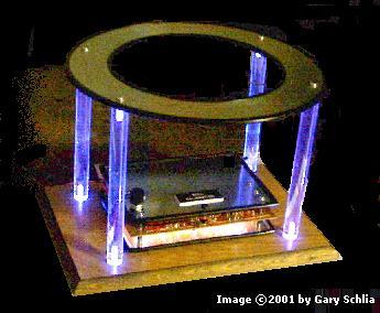
Photo Courtesy of Gary Schlia
Kynar® is a registered trademark of Elf Atochem North America, Inc.
Teflon® is a registered trademark of E. I. du Pont de Nemours and
Company.
Wire-Wrap® is a registered trademark of Cooper Industries, Inc.
Text and drawings ©1999, 2002, 2014. 2017, 2018 by Arthur Harrison
Parts list updated 20181104