The 203 Theremin
A Battery-Operated Version of the Wien-Bridge Theremin
September 22, 2001
Updated May 22, 2002
Contents
Legal Notice
Safety Notices
Introduction
Assembly Procedure
Calibration Procedure
Schematic
Circuit Description
Parts Table
Drawing
Index
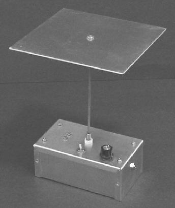
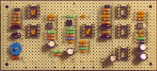
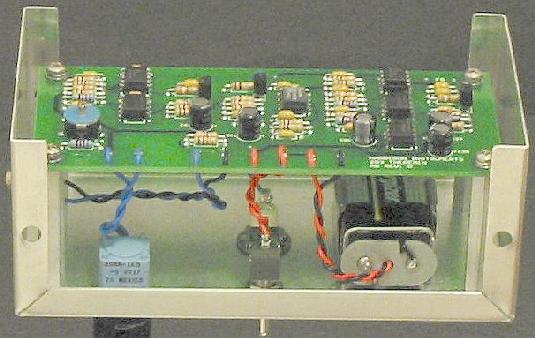
Photos
Legal Notice
(back to contents)
The information contained in this document is ©2001 by Arthur Harrison. Any reproduction of the information contained in this document, electronic or mechanical, shall only be used with Arthur Harrison's permission, and shall acknowledge him as the copyright holder and author.
Use of the information contained in this document for personal or commercial financial gain, such as the manufacture and sale of electronic musical instruments or parts thereof, is prohibited. Unless specifically stated in a written contract, Arthur Harrison grants no licence for the commercial exploitation of the concepts and designs embodied in this document. Refer licensing inquiries to: theremin1@worldnet.att.net.
The information contained in this document may only be reproduced in small quantities when the purpose for its use is the dissemination of information to students or hobbyists, and may not be distributed in any form, electronic or mechanical, for the purposes of any party engaged, directly or indirectly, in commercial enterprises.
Arthur Harrison assumes no liability for any damages, direct, or consequential,
which may arise from the dissemination, application, or misapplication of
the content contained in this site. The User of the information provided
in this site assumes all responsibility for any damages, direct or consequential,
which may arise from its use. Arthur Harrison retains the right to alter
the content within this site at any time without notice.
Safety Notices
(back to contents)
DANGER: Do not play this instrument at a high volume, especially when using headphones. Use headphones that have a built-in volume control, and adjust the volume control for a comfortable level. Hearing experts advise against the continuous, extended use of headphones.
DANGER: Some of the components used in this construction are "polarized," which means that they will only function properly when inserted into the circuit in the right direction. Always observe component polarities carefully, and double-check the orientation of transistors, diodes, integrated circuits and polarized capacitors before applying power to any circuit. Do not reuse a part which has been subjected to improper insertion.
DANGER: Wear safety glasses and use all appropriate
safety equipment when working with tools and materials. Always follow safe
shop practices and obey safety rules.
Introduction
(back to contents)
The 203 Theremin utilizes Wien-bridge oscillators in a heterodyne configuration to produce an audible tone that corresponds to hand position. The instrument provides the convenience and safety of 9-volt battery operation, in a compact enclosure. It is a pitch-only theremin, primarily intended for use with an external amplifier and speaker, although it has sufficient output power to drive headphones directly.
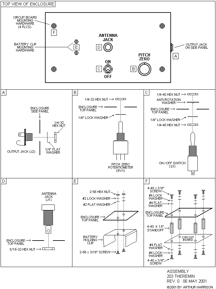
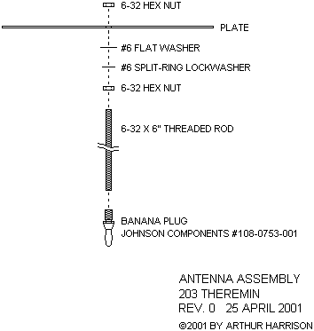
A jack on the top of the unit accepts the antenna assembly that consists of a support rod and a 6-inch-square metal plate. An on-off switch and a pitch zero control are located on the top panel, and a 1/8th-inch monophonic phone jack for the output is located on the side.
A note regarding external interference: The 203 Theremin is prone to interference from sources such as power lines, fluorescent lighting fixtures, incandescent lamp dimmers, and computers. Such sources will cause modulation of the instrument's output tone that may render it unsuitable for certain applications where high fidelity is required. In some cases, effects from interfering sources may be remedied by moving the theremin to a different area.
Where absolute assurance of fidelity is not an issue, the 203 Theremin is highly suitable as a practice and demonstration instrument, due to its portability, excellent stability, and pleasing tone quality. The MP3 sound sample below was recorded under typical conditions. Your results may vary.
| 203 Theremin Wave |
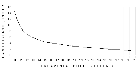
The following graph illustrates the approximate relationship of pitch and hand distance for a 203 theremin, when constructed and calibrated as specified in this article:
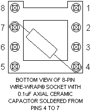
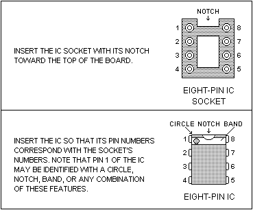
The builder has two options for the 203 Theremin circuit board:
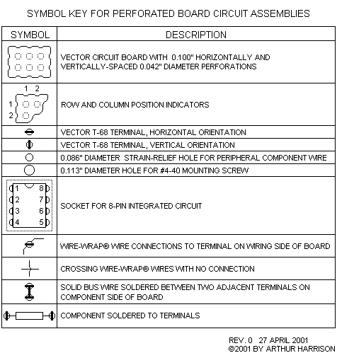
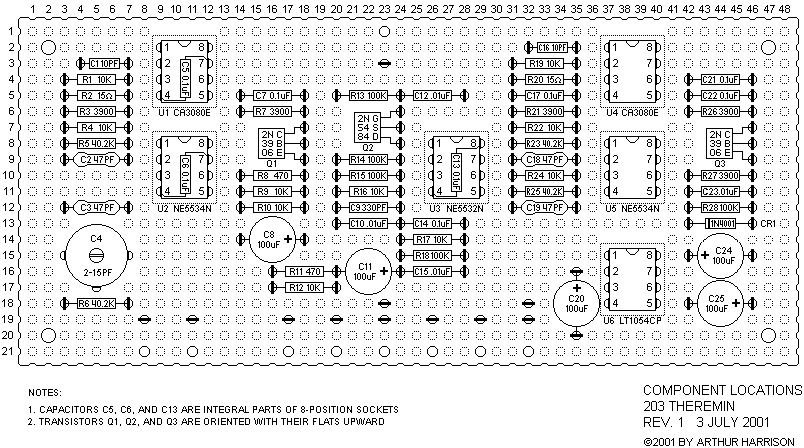
As in previous articles, I have supplied detailed lay-out drawings for the circuit using Vector perforated board and Wire-Wrap® terminals and sockets. To obtain a compact form-factor, this circuit lay-out is dense, requiring an advanced level of construction skill.
Alternatively, a complete printed circuit board, fully populated and tested, is available. The printed circuit board and the Wire-Wrap® board both have the same mounting-hole locations and the same wire connection pattern, and will function identically. The printed circuit version has the advantage of reduced height, since there are no terminal pins extending from the bottom of the board. Builders may find more economy in purchasing the printed circuit board instead of all the components separately, and enduring the labor-intensive task of component soldering and wire-wrapping.
See ordering information for the 203 Theremin printed circuit board at: |
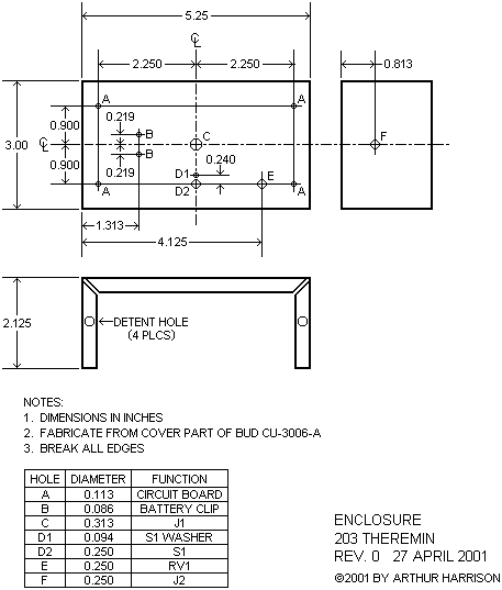
This article also includes details to fabricate the theremin's enclosure and antenna assembly. Alternatively, builders may devise their own.
For those who prefer additional construction guidance, I have included an
"Assembly Procedure" section with step-by-step instructions for fabricating
the 203 Theremin.
Assembly Procedure
(back to contents)
If you have the printed circuit board, then use the
Alternative Assembly Procedure.
Otherwise, use the following procedure to fabricate both the Wire-Wrap®
board and the enclosure.
Calibration Procedure
(back to contents)
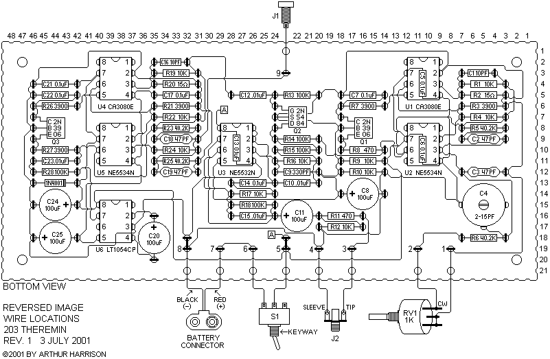
Schematic for the 203 Theremin
(back to contents)
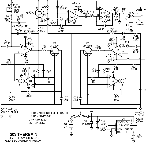
Circuit Description
(back to contents)
The 203 Theremin uses two Wien-bridge oscillators, one fixed in frequency, and the other that has a frequency influenced by hand capacitance in the proximity of its antenna. It is the difference frequency between the two, obtained with heterodyning, that provides the theremin's audible tone. Wien-bridge oscillators were chosen for their good temperature stability and moderate immunity from electromagnetic and radio frequency interference. In addition, they do not require obscure air-core inductors.
The fixed-frequency oscillator is comprised of operational amplifier U2 and the frequency-determining elements in its Wien network; C2, R5, C3, and R6. Variable components C4 and RV1, also part of the Wien network, provide a means of adjusting the frequency so that a zero beat condition can be obtained when the hand is away from the antenna. The frequency of oscillation is described by the equation 1/2piRC, where R=R5=R6 and C=C2=C3. This equation yields a frequency of about 84kHz, although in practice, the actual frequency will be somewhat lower due to the addition of the two variable components and stray circuit capacitance.
Resistors R9 and R10, and capacitor C8 provide a one-half-supply reference for the oscillator. Resistor R8 converts the oscillator's output voltage into a current. Transistor Q1 provides half-wave rectification of this current, and permits it to be negative-rail referenced, as required by U1, an operational transconductance amplifier (OTA). Resistor R7 and capacitor C7 provide an averaged value of this current to the OTA's amplifier bias control input (pin 5).
The OTA's positive input is fed from the oscillator's output, substantially attenuated by R1 and R2 to prevent non-linearities in its transfer function. The OTA's output feeds the negative input of U2. The criteria for oscillation is that the inverting gain of the operational amplifier be exactly 2. This gain is partly determined by the ratio of R4 and R3, which, in itself, is greater than 2. However, a path parallel to R4, via the OTA, reduces this ratio according to the current at its amplifier bias control input (pin 5).
As Q1's collector voltage rises, the OTA's transconductance increases, effectively increasing the oscillator's negative feedback, and thus reducing the amplitude of oscillation, until the base-emitter junction of Q1 falls below the threshold of conduction. This, in turn, lowers Q1's collector voltage, sustaining oscillation. The output amplitude is primarily a function of Q1's base-emitter voltage and the value of R8.
Capacitor C1 suppresses out-of-band high-frequency components at the output of U2. Capacitors C5 and C6 provide decoupling for U1 and U2, respectively. The sine-wave amplitude at U2's output (pin 6) is between 2 and 3.5 volts peak-to-peak, centered about +4.5 volts. This amplitude is affected by the two variable components, C4 and RV1. Note that strict regulation of the oscillator amplitude with variations in the Wien network is not a criteria in this circuit; the amplitude control loop only satisfies the requirement that oscillation is sustained and remains sinusoidal for all values of C4 and RV1.
The variable oscillator, comprised of operational amplifier U5, OTA U4, and transistor Q3, is essentially identical to the fixed-frequency oscillator. Antenna A1 provides a means of frequency modulation for the oscillator with hand capacitance. Resistor R24 protects U5's input from static discharges. Charge-pump voltage inverter U6 and associated components develops a negative supply bias that approximately doubles the battery voltage to the oscillator. The increased supply voltage permits a large sine-wave voltage amplitude at the antenna, required for adequate signal-to-noise performance of the theremin. Although the charge pump is capable of self-oscillation, this is avoided to prevent unwanted audible frequency products. Instead, the charge-pump waveform is synchronously controlled by the variable oscillator via C23 and R28. The sine-wave amplitude at U5's output (pin 6) is about 13 volts peak-to-peak, centered about ground, with the antenna disconnected. This value drops to about 8 volts peak-to-peak, with the antenna inserted. The variable oscillator output voltage is determined by the value of R27, and was selected to ensure a sine-wave output with the lowest practical battery voltage.
The fixed-frequency oscillator's output is applied to R14. The output from the local oscillator is applied to the gate of Q3, a depletion-mode, N-channel, junction field-effect transistor, via C12. The levels at Q2’s gate are reestablished symmetrically about the one-half-supply reference (AC ground) via R13. With Q3's gate positive in respect to its source, it turns on, shunting the signal at the junction of R14 and R15 to AC ground. With the gate negative, Q3 turns off, allowing the signal to be present at R15. Heterodyning, which results from the gating of the fixed-frequency oscillator output by the variable oscillator output, takes place at the junction of R14 and R15.
U3A, in conjunction with R14, R15, R16, C9, and C10, form a Sallen-Key low-pass filter that removes the sum frequency from the heterodyne process, leaving the audible difference frequency. The output of the filter is AC coupled via C14 to an inverting gain stage consisting of U3B and associated components. R17 and R18 establish the dc gain for this stage. C15, in conjunction with R18, determine the U3B stage's high-frequency roll-off, and C14, in conjunction with R17, establish its low-frequency roll-off. The combined low-pass functions of the Sallen-Key and U3B sections result in an audio output that has constant loudness over the instrument's 20 to 2500Hz range. Capacitor C11 blocks DC from the output, resistor R12 discharges C11 to prevent residual charges from causing audio transients, and resistor R11 isolates U3B’s output from load capacitance and serves as a current limiter. Capacitor C13 provides decoupling for U3.
The output wave shape is essentially sinusoidal from 100Hz to the terminal frequency, with a maximum amplitude of about 2.8 volts, peak-to-peak occurring at about 180Hz. Below 100Hz, the output wave-form exhibits substantial, although pleasing, harmonics that result from oscillator coupling. The circuit produces about 15 millivolts peak-to-peak of noise, measured at zero-beat, yielding a signal-to-noise ratio of 44dB. This ratio, however, may be degraded due to external interference, which will vary considerably depending on the instrument's proximity to emissive sources such as power lines, fluorescent lighting fixtures, incandescent lamp dimmers, and computers.
The oscillators exhibit excellent frequency immunity to supply variations, with only 0.04 percent change from 6 to 9.5 volts. This supply voltage immunity, in addition to first-order cancellation between the two similar oscillators, permits circuit operation without input voltage regulation. Current consumption from a 9-volt battery is approximately 23 milliamperes, and the circuit will operate with no performance compromise down to 6 volts, thereby extending battery life considerably.
Parts Table
(back to contents)
DISTRIBUTOR LINKS
Mouser |
http://www.mouser.com/ |
Allied |
http://www.alliedelec.com/ |
Digi-Key |
http://www.digikey.com/ |
McMaster-Carr |
http://www.mcmaster.com/ |
| ITEM | DESCRIPTION | VALUE | MANUFACTURER | MANUFACTURER PART NUMBER |
SUPPLIER | SUPPLIER STOCK NUMBER |
QTY |
| A1 (NOTE 1) |
ANTENNA | . | . | . | . | . | 1 |
| B1 | BATTERY | 9 VOLT, NEDA 1604 |
EVEREADY | 522 | MOUSER | 525-522 | 1 |
| C1,C16 | CERAMIC CAPACITOR |
10pF, +/-5%, NPO, 100V, AXIAL |
KEMET | C410C100J1G5CA | MOUSER | 80-C410C100J1G | 2 |
| C2,C3, C18,C19 |
MICA CAPACITOR |
47pF, +/-5%, 300V, RADIAL |
CORNELL DUBILIER |
EC470J03 | MOUSER | 5982-5-300V47 | 4 |
| C4 | POLYPROPYLENE VARIABLE CAPACITOR |
2 TO 15 pF | SPRAGUE/ GOODMAN |
GYC15000 | DIGI-KEY | SG3006-ND | 1 |
| C5,C6, C7,C13, C14,C17, C21,C22 |
CERAMIC CAPACITOR |
0.1 uF, +/-10%, X7R, 50 V, AXIAL |
KEMET | C412C104K5R5CA | MOUSER | 80-C412C104K5R | 8 |
| C8,C11, C20,C24, C25 |
ALUMINUM ELECTROLYTIC CAPACITOR |
100 uF +/-20%, 16 V, RADIAL, 6.3mm D x 7mm L, 2.5mm LEAD SPACE |
NICHICON | USR1C101MDA | MOUSER | 647-USR1C101MDA | 5 |
| C9 | CERAMIC CAPACITOR |
330pF, +/-5%, COG, 50 V, AXIAL |
KEMET | C410C331J1G5CA | MOUSER | 80-C410C331J1G | 1 |
| C10,C12, C15,C23 |
CERAMIC CAPACITOR |
0.01uF, +/-10%, X7R, 50 V, AXIAL |
KEMET | C410C103K5R5CA | MOUSER | 80-C410C103K5R | 4 |
| CR1 | RECTIFIER | 1A, 50V, AXIAL |
RECTRON | 1N4001 | MOUSER | 583-1N4001 | 1 |
| J1 | BANANA JACK, ANTENNA |
INSULATED, NYLON, WHITE, 5/16"-32 UNEF-2A THREAD |
JOHNSON COMPONENTS |
108-0901-001 | MOUSER | 530-108-0901-1 | 1 |
| J2 | JACK, OUTPUT |
MONO, 1/8" | SWITCHCRAFT | 42A | MOUSER | 502-42A | 1 |
| P1 | BANANA PLUG, ANTENNA |
UNINSULATED, 6-32 INTERNAL THREAD, 0.175" ACROSS FLATS |
JOHNSON COMPONENTS |
108-0753-001 | MOUSER | 530-108-0753-1 | 1 |
| Q1,Q3 | TRANSISTOR | PNP, TO-92 CASE |
CENTRAL SEMICONDUCTOR |
2N3906 | MOUSER | 610-2N3906 | 2 |
| Q2 | JUNCTION FIELD EFFECT TRANSISTOR |
N-CHANNEL | CENTRAL SEMICONDUCTOR |
2N5484 | MOUSER | 610-2N5484 | 1 |
| R1,R4, R9,R10, R12,R16, R17,R19, R22,R24 |
RESISTOR, CARBON FILM |
10K OHM +/-5%, 1/4 WATT |
XICON | 29SJ250-10K | MOUSER | 291-10K | 10 |
| R2,R20 | RESISTOR, CARBON FILM |
15 OHM +/-5%, 1/4 WATT |
XICON | 29SJ250-15 | MOUSER | 291-15 | 2 |
| R3,R7, R21,R26, R27 |
RESISTOR, CARBON FILM |
3900 OHM +/-5%, 1/4 WATT |
XICON | 29SJ250-3.9K | MOUSER | 291-3.9K | 5 |
| R5,R6, R23,R25 |
RESISTOR, METAL FILM |
40.2K OHM +/-1%, 1/4 WATT |
XICON | 271-40.2K | MOUSER | 271-40.2K | 4 |
| R8,R11 | RESISTOR, CARBON FILM |
470 OHM +/-5%, 1/4 WATT |
XICON | 29SJ250-470 | MOUSER | 291-470 | 2 |
| R13,R14, R15,R18, R28 |
RESISTOR, CARBON FILM |
100K OHM +/-5%, 1/4 WATT |
XICON | 29SJ250-100K | MOUSER | 291-100K | 5 |
| RV1 | POTENTIOMETER | 1K OHM +/-10%, LINEAR TAPER, CONDUCTIVE PLASTIC, 1/8" SHAFT |
INVENSYS/ CLAROSTAT |
392JB1K | DIGI-KEY | 392JB102-ND | 1 |
| S1 | SWITCH | SPDT | ITT INDUSTRIES/ C & K |
7101SYZQE | MOUSER | 611-7101-001 | 1 |
| U1,U4 | INTEGRATED CIRCUIT |
OPERATIONAL AMPLIFIER, 8-PIN DIP PACKAGE |
PHILLIPS SEMICONDUCTORS |
NE5534N | ALLIED | 236-0298 | 2 |
| U2,U5 | INTEGRATED CIRCUIT |
OPERATIONAL TRANSCONDUCTANCE AMPLIFIER, 8-PIN DIP PACKAGE |
INTERSIL | CA3080E | ALLIED | 903-0286 | 2 |
| U3 | INTEGRATED CIRCUIT |
DUAL OPERATIONAL AMPLIFIER, 8-PIN DIP PACKAGE |
PHILLIPS SEMICONDUCTORS |
NE5532N | ALLIED | 236-0286 | 1 |
| U6 | INTEGRATED CIRCUIT |
VOLTAGE INVERTER, 8-PIN DIP PACKAGE |
TEXAS INSTRUMENTS |
LT1054CP | ALLIED | 735-3681 | 1 |
| . | SOCKET FOR INTEGRATED CIRCUIT |
8-POSITION, WIRE-WRAP®, OPEN FRAME |
MILL-MAX | 123-93-308-41-001 | MOUSER | 575-293308 | 6 |
| . | PERFORATED BOARD |
GLASS-EPOXY, 6.5" X 4.5" X 0.062" |
VECTOR | 64P44WE | MOUSER | 574-64P44WE | 1 |
| (NOTE 2) | TERMINAL | PRESS-FIT, SOLDER FORK TO WIRE-WRAP® |
VECTOR | T68 | MOUSER | 574-T68/C | 2 |
| . | KNOB, POTENTIOMETER | 0.740"D, 0.437"H, FOR 0.125"D SHAFT |
TYCO/ AUGAT |
PKES-60B-1/8 | ALLIED | 759-1110 | 1 |
| . | STANDOFF, CIRCUIT BOARD SUPPORT |
4-40 THREAD, 1.5" LONG, HEXAGONAL, ALUMINUM |
KEYSTONE | 2206 | MOUSER | 534-2206 | 4 |
| . | CONNECTOR, 9 VOLT BATTERY |
. | KEYSTONE | 2241 | DIGI-KEY | 2241K-ND | 1 |
| . | MOUNTING CLIP, 9 VOLT BATTERY |
. | KEYSTONE | 71 | MOUSER | 534-71 | 1 |
| . | MACHINE SCREW, BATTERY CLIP MOUNTING |
PAN HEAD, PHILLIPS, 2-56 X 3/16" STAINLESS STEEL |
. | . | MCMASTER- CARR |
91772A105 | 2 |
| . | FLAT WASHER, BATTERY CLIP MOUNTING |
#2, 0.25" O.D., STAINLESS STEEL |
. | . | MCMASTER- CARR |
98019A300 | 2 |
| . | LOCK WASHER, BATTERY CLIP MOUNTING |
#2 SPLIT-RING, 0.172" O.D., STAINLESS STEEL |
. | . | MCMASTER- CARR |
92146A520 | 2 |
| . | NUT, BATTERY CLIP MOUNTING |
2-56 X 0.188, STAINLESS STEEL |
. | . | MCMASTER- CARR |
91841A003 | 2 |
| (NOTE 3) | WIRE, HOOK-UP | 22 GAUGE, STRANDED, TEFLON INSULATED, WHITE |
ALPHA | 5855-100-01 (ROLL OF 100') |
MOUSER | 602-5855-100-01 (ROLL OF 100') |
1 |
| (NOTE 4) | WIRE, WIRE-WRAP® | 26 GAUGE, SOLID, KYNAR INSULATED, BLACK |
OK INDUSTRIES | R26BLK-0100 (ROLL OF 100') |
DIGI-KEY | K386-ND (ROLL OF 100') |
1 |
| . | MACHINE SCREW, CIRCUIT BOARD MOUNTING |
PAN HEAD, PHILLIPS, 4-40 X 3/8", STAINLESS STEEL |
. | . | MCMASTER- CARR |
91772A108 | 8 |
| . | FLAT WASHER, CIRCUIT BOARD MOUNTING |
#4, 0.25" O.D., STAINLESS STEEL |
. | . | MCMASTER- CARR |
98019A309 | 8 |
| . | LOCK WASHER, CIRCUIT BOARD MOUNTING |
#4 SPLIT-RING, 0.12" O.D., STAINLESS STEEL |
. | . | MCMASTER- CARR |
92146A530 | 8 |
| . | ENCLOSURE | 2 PIECE, 5.25" WIDE X 3" HIGH X 2.125" DEEP, ALUMINUM |
BUD | CU-3006-A | ALLIED | 736-3657 | 1 |
| . | THREADED ROD, ANTENNA SUPPORT |
6-32 THREAD, 2' LONG STAINLESS STEEL |
. | . | MCMASTER- CARR |
98804A007 | 1 |
| . | NUT, ANTENNA SUPPORT |
6-32 X 5/16" STAINLESS STEEL |
. | . | MCMASTER- CARR |
91841A007 | 2 |
| . | FLAT WASHER, ANTENNA SUPPORT |
#6, 0.312" O.D., STAINLESS STEEL |
. | . | MCMASTER- CARR |
98019A314 | 1 |
| . | LOCK WASHER, ANTENNA SUPPORT |
#6 SPLIT-RING, 0.25" O.D., STAINLESS STEEL |
. | . | MCMASTER- CARR |
92146A540 | 1 |
Notes:
The cost of the items in the parts list, tabulated on May 25, 2001, was $91.33.
The actual procurement cost will be higher due to minimum purchase requirements
for some items (see the following notes).
The value of the ANTENNA was given as $4.00.
The value of Mouser RESISTORS, which are sold in minimums of 10 per type,
were calculated per piece. Procurement cost for all resistors except Mouser
291-10K (10 used) will be higher due to the minimum purchase requirement.
The value of the PERFORATED BOARD (Mouser 574-64P44WE) was calculated based
on the unit cost, regardless of unused excess.
The value of the TERMINALS (Mouser 574-T68/C) was calculated based on the
unit cost, regardless of unused excess.
The value of the WIRE, HOOKUP (Mouser 602-5855-100-01) was calculated based
on the average requirement of 4 feet per unit. Procurement cost for this
item will be higher due to the minimum purchase requirement.
The value of the WIRE, WIRE-WRAP® (Mouser 602-5855-100-01) was calculated
based on the unit cost, regardless of unused excess.
The value of the THREADED ROD, ANTENNA SUPPORT, was calculated based on the
unit cost, regardless of unused excess.
The value of McMaster-Carr MACHINE SCREWS, FLAT WASHERS, LOCK WASHERS and
NUTS, which are only sold in bulk, were calculated per piece. Procurement
cost for these items will be higher due to the minimum purchase
requirements.
Drawing Index
(back to contents)
|
|
|
Kynar® is a registered trademark of Elf Atochem North America, Inc.
Teflon® is a registered trademark of E. I. du Pont de Nemours and
Company.
Wire-Wrap® is a registered trademark of Cooper Industries, Inc.
Text, drawings, and photographs ©2001 by Arthur Harrison
|
THE "203 THEREMIN" |