|
THE GLASGOW DIGITAL THEREMIN
Published November 4, 2003
Introduction
This theremin was built by students at the University of Glasgow for their physics course. The students presented two theremin circuits, one called an "Analog Theremin," and the other a "Digital Theremin," the latter of which is described here. Prompted by many inquiries from theremin constructors, the purpose of this article is to present a clearer, redrawn schematic in which I have corrected some minor errors and substituted obsolete ICs with currently-available types. I have made no attempt to modify the original design, other than to provide a few changes that I deemed necessary for correct functionality consistent with the original designers' intentions. I have also included a basic analysis of the circuit.
The circuit was originally published by Kenneth D. Skeldon, Lindsay M. Reid, Viviene McNally, Brendan Dougan and Craig Fulton in the November, 1998 issue of American Journal of Physics, in an article titled "Physics of the Theremin," (Volume 66, Number 11, page 945.)
Dr. Skeldon has kindly consented to answering inquiries about the instrument, and he may be contacted at ken@seidam.com.
Terminology
There is a popular notion that separates theremin designs into two categories, "analog" and "digital." Often, this distinction is really referring to the types of components in the theremin, and not necessarily its overall operating principle. In Leon Theremin's original design, for example, the pitch is generated by applying the outputs of two radio-frequency oscillators to a mixer, and then filtering the mixer's output to obtain the audible beat frequency. He implemented these functions with two triode vacuum-tube oscillators and a tetrode vacuum-tube mixer. While a more recent design may substitute the triode oscillators with NAND gates and the mixer with an EXCLUSIVE-OR gate, the actual principles of operation remain essentially similar to the older vacuum tube design. The gates are considered "digital" devices because (ignoring transitions) they produce an output which is either a high (logical "1") state or a low (logical "0") state, but the prevailing, overall mode of operation is unchanged from Theremin's original design.
The Glasgow Digital pitch circuit is distinguished from the original theremin, however, in that the mixer's output is further processed by a frequency-to-voltage converter (tachometer) followed by a voltage-controlled oscillator (VCO). Thus, its audible output is not the direct heterodyne of the two radio-frequency oscillators, but a derivative of the heterodyne. The volume scheme also departs from the original, in that it uses a process identical to the pitch scheme, except substituting a voltage-controlled amplifier (VCA) for the VCO.
Circuit Analysis
Pitch Section
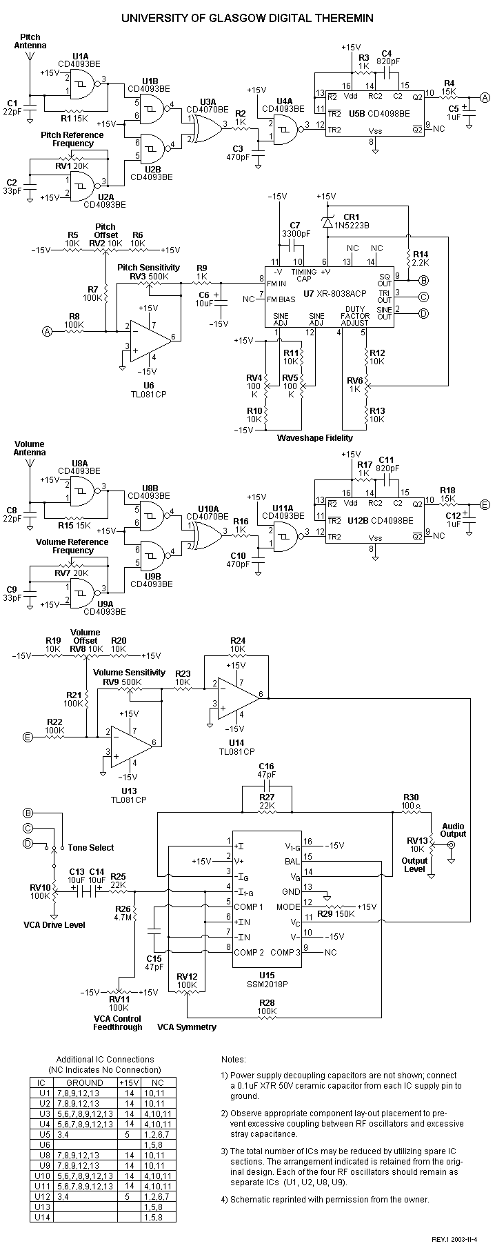
Referring to the schematic the pitch section is examined first. NAND gate U1A, configured as a hysteretic inverter, forms a relaxation oscillator in which the output frequency is determined by R1, C1, and also the capacitance between the hand and the pitch antenna. It is therefore called the "hand oscillator." As the hand moves closer to the antenna, the total capacitance increases, causing the oscillator's output frequency to decrease. Section U1B, another inverter-configured NAND gate, isolates the hand oscillator from loading effects.
NAND GATE U2A, configured as a hysteretic inverter, forms a relaxation oscillator in conjunction with RV1 and C2, which determines its frequency. The output frequency of this oscillator is initially adjusted with RV1 for a fixed frequency, so it is called the "reference oscillator." Section U2B, another inverter-configured NAND gate, isolates the reference oscillator from loading effects. The outputs of the two oscillators are applied to the inputs of EXCLUSIVE-OR (XOR) gate U3A.
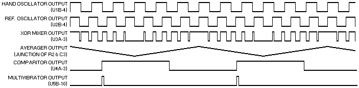
The pitch circuit's operation is represented in the figure below. The outputs of the oscillators, given a fixed hand distance, are two non-synchronized square waves with different frequencies. The XOR gate produces a high (logical "1") state when both of its inputs are equivalent, and a low (logical "0") state when its inputs are different. The XOR's output is applied to an R-C averaging circuit consisting of R2 and C3, which smoothes the progression of logic states into a triangular-like waveform with a frequency equal to the difference frequency between the two oscillators. As the hand comes closer to the pitch antenna, the hand oscillator's output decreases, causing the frequency of the waveform at the averager's output to increase.
|
Next, the averager's waveform is applied to inverter-configured NAND gate U4A. This gate converts the triangular-like waveform into a square wave of the same frequency. The square wave is then applied to a tachometer circuit as follows: U5B, a monostable multivibrator, produces a fixed-width pulse at its output each time its input transitions from a low-to-high state. The pulse train is then averaged by R4 and C5 which provides a DC voltage that is proportional to the oscillators' difference frequency. U5B's output pulse width is set by R3 and C4.
The tachometer output voltage (point "A" in the schematic) is amplified and offset by operational amplifier U6 and associated components so that it is compatible with voltage-controlled oscillator (VCO) U7's input. R9 and C6 provide additional filtering to reduce residual AC components at the VCO's input to a negligible value. In use, Pitch Offset potentiometer RV2 and Pitch Sensitivity potentiometer RV3 are adjusted so that the voltage applied to U7's input spans from about +12.5V to +4.2V, corresponding to an audio frequency range of about 100Hz to 12kHz for a hand distance ranging from about 18 inches to 1 inch.
U7 is a waveform generator with a voltage-controlled frequency (FM) input and outputs that include sine, triangle, and square waves. U7's output frequency is determined by the value of C7 and the currents flowing through R12 and R13. The resistor currents are determined by the voltage applied to FM input pin 8.
The FM input voltage is measured with respect to the voltage at positive supply pin 6. To obtain the lower portion of the sweep range, The FM input voltage must exceed the positive supply voltage by several hundred millivolts. Accordingly, 2.7v zener diode CR1 is used to lower U7's positive supply to approximately +12.3v. The sweep range, therefore, starts at approximately +12.3v. Lowering U7's positive supply is also beneficial with regard to operational amplifier U6's positive output limit, which is typically 1.5v below its positive supply.
The allowable sweep input voltage ranges from Vpin6 for no waveform output to (1/3 Vpin6)-2v for maximum output frequency. A minor insufficiency in U7's design causes the waveform outputs to initiate at about 100Hz when rising, and end at about 10Hz when falling.
Three potentiometers are used to trim U7's output waveshapes. VR6 adjusts the triangle for equal slopes, and VR4 and VR5 adjust the sine waveform's vertical symmetry. In practice, the waveforms may be intentionally set for asymmetry, depending on the desired tone quality.
Volume Section
The theremin's volume section is nearly identical to the pitch section. U8A serves as the hand oscillator, with U8B as an isolation buffer. U9A serves as the reference oscillator, with U9B as an isolation buffer. The outputs of these two oscillators are mixed at XOR gate U10A, applied to R-C averager R16-C10, and then applied to inverter-configured NAND gate U11A, which converts the waveform into a square wave. The square wave is then applied to a tachometer consisting of monostable multivibrator U12B, R18, and C12. R17 and C11 set U12B's output pulse width.
The tachometer output voltage (point "E" in the schematic) is amplified and offset by operational amplifier U13 and associated components, and inverted by U14 and associated components so that it is compatible with the U15's Vc input (pin 11). The gain of the VCA, and therefore the output volume, decreases 1dB per 30mV increase at the Vc pin. The volume decreases as the hand is moved toward the antenna, a property which is consistent with original theremins.
One of three waveforms from VCO U7 is selected by switch S1 and provided to the U15's -I1-G input (pin 4). This input is connected to a virtual ground node within the IC, and resistor R25 converts the input waveform voltage into current. Capacitors C13 and C14 are used to minimize the DC offset voltage caused by bias current flowing through R25 and also assure that any DC offset voltage from the VCO is eliminated. Note that each of the waveforms have different amplitudes; the square wave being 30v P-P, the triangle 9v P-P and the sine 6v P-P. Accordingly, RV10 is used to adjust the drive level to U15's -I1-G input for 2.0v P-P.
RV11 is adjusted to eliminate slight offset variations caused by the volume control voltage. In practice, it is set so that no DC offset occurs as the volume control voltage varies over its full range. If desired, RV11 and R26 can be eliminated, since the offset variations (caused by volume hand movement) are very small and not within the audible range. (See: "Obsolescence.")
C15 is a frequency compensation capacitor to prevent U15 from oscillating. R29 sets the current in U15's gain core, adjusting the amount of "class B" current, which optimizes the device's noise and distortion performance. R27 and C16 set the gain and high-frequency rolloff of U15's output stage. R30 isolates U15's output from excessive capacitive loads that may cause instability. RV13 is the output level control. U15's pin 16 is an unused output from one of its internal amplifiers. It is connected to the negative supply, which disables that amplifier to prevent oscillations.
Power Amplifier
The original design has an obsolete National Semiconductor LM759 output amplifier for driving headphones, not shown in the new schematic. The SSM2018P's output has a low impedance capable of driving about ±1.3mA, which is sufficient for many audio amplifier inputs. If greater loads have to be driven directly from the theremin, an appropriate on-board amplifier may be added.
Performance
A breadboard of the theremin with 5.5 inch by 8 inch antenna plates provided the following values:
| Hand oscillator frequency | U1B-4 | 1.19MHz to 1MHz |
| Reference oscillator frequency | U2B-4 | 1.2MHz |
| Multivibrator output frequency | U5B-10 | 10KHz to 200kHz |
| Multivibrator output pulse width | U5B-10 | 0.9uS |
| Tachometer output voltage | A | +0.135v to +2.7v |
| VCO input voltage | U7-8 | +12.5v to +4.2v |
| VCO output frequency | U7-9 | 100Hz to 12kHz |
| Hand oscillator frequency | U8B-4 | 1.19MHz to 1MHz |
| Reference oscillator frequency | U9B-4 | 1.2MHz |
| Multivibrator output frequency | U12B-10 | 10KHz to 200kHz |
| Multivibrator output pulse width | U12B-10 | 0.9uS |
| Tachometer output voltage | E | +0.135v to +2.7v |
| VCA control input voltage | U15-11 | -0.5v to +1v |
| VCA drive level | RV10 slider | 2v P-P |
| Audio output | J1 tip | 12v P-P to 0v |
Obsolescence
The source document specifies operational amplifiers U6, U13, and U14 as "TLE2027." The inexpensive plastic dual-inline package version of this part, Texas Instruments TLE2027CP, is obsolete. Ceramic dual-inline versions are still available as Texas Instruments types TLE2027MJG and TLE2027MJGB, but they are expensive and tend to require large minimum-quantity purchases. The Texas Instruments TL081CP is an inexpensive, widely-available alternative which functions equally well in this application.
The source document specifies waveform generator U7 as "8038." Either the Intersil type ICL8038CCPD, or the Exar XR-8038A will function in this circuit. Both are plastic dual-inline package parts.
The source document specifies VCA U14 as "SSM-2018." Either the Analog Devices type SSM2018P or SSM2018TP will function in this circuit. The SSM2018TP is the "trimless" version. If this version is used, then RV11, RV12, and R26 may be omitted from the circuit.
Text and drawing ©2003 Arthur Harrison. The theremin schematic was
used
with the permission of its owners.
Contact Author
Back to Art's Theremin Page